Chapter 3 - System Overview
3.1 - OVERVIEW
The Kurzweil 250 models are electro-mechanical instruments. They generate sound by a combination of mechanical and electrical functions. This section first presents an overview of the instruments and then describes each sub-system as a whole. Each of the three Kurzweil 250 models are described under their specific headings.
3.1.1 - Kurzweil 250
The Kurzweil 250's hardware is divided into two modules, the enclosure and the POD. The enclosure contains the piano keyboard and most of the system's electronics. The POD contains the power supply and the foot pedals.
The enclosure usually rests on its stand. The POD sits on the floor and is connected to the enclosure by a large harness cable.
The user has two main ways to control the instrument, through the piano keyboard (primarily during performance) and through the front control panel (mostly during "setup" before a performance).
3.1.2 - Kurzweil 250X
The Kurzweil 250X's hardware is also divided into two modules, the enclosure and POD. The enclosure contains most of the system's electronics. The POD contains the power supply. The POD sits on the floor and is connected to the enclosure by a large harness cable.
3.1.3 - Kurzweil RMX 250 AND 225
The hardware for the Kurzweil RMX is in its self-contained, rack mount enclosure. Unlike the K250 and K250X, the power supply is internally mounted in the RMX module.
3.2 - MECHANICAL OVERVIEW
3.2.1 - Kurzweil 250 Enclosure Overview
The enclosure is molded in two parts, a top and bottom.
Figure 3.1
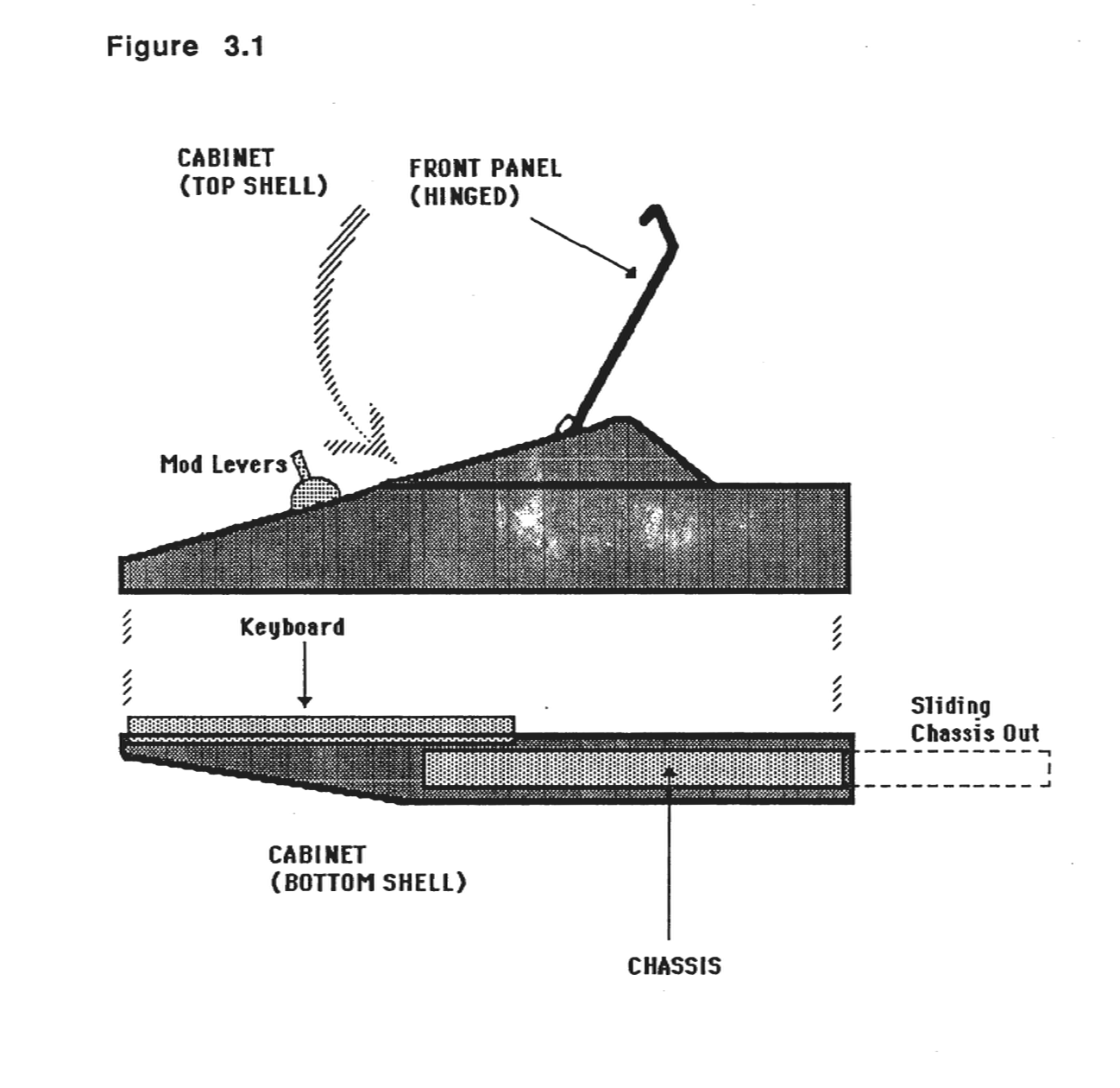
Inside the enclosure there are three major sub-assemblies:
*The Chassis Sub-assembly
*The Keyboard Sub-assembly
*The Front Panel Sub-assembly*
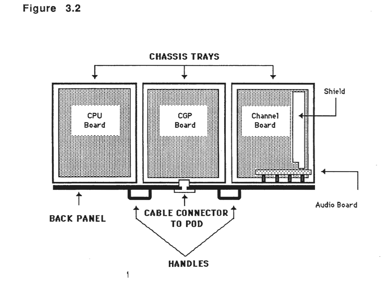
Chassis Sub-Assembly
The chassis sub-assembly is a metal tray which slides out from the back of the instrument for servicing. The chassis is divided into three compartments, each cradling a large circuit board. Most of the circuitry in the system is on the three large boards. The boards are the Central Processing Unit (CPU), the Channel Group Processor (CGP) and the Channel board. The chassis also contains a small board, the Audio board, mounted inside the back panel. These boards are described in detail later.
Figure 3.2
Front Panel Sub-Assembly
The Front Panel sub-assembly of the Kurzweil 250 and the Kurzweil 250X has three board mounted on the faceplate. They are the following:
Slider board
Control Panel board
LCD board
The Slider board contains circuitry for the continuous (smooth-panning) controls. The Control Panel board controls the on/off operation of the 55 buttons and the 38 LEDs. The Control Panel also contains an analog/digital converter (ADC) that translates the analog signals into digital values. The LCD board controls the liquid crystal display which shows numbers and text.
The Front Panel sub-assembly of the Kurzweil RMX has one board mounted on the faceplate. The assembly is referred to as the RMX Control Panel board.
POD Assembly (K250 and K250X only)
The POD contains the power supply and the piano-style foot pedals. Most of the bulk of the POD is the power supply.
The POD contains a 5 volt supply for the system's logic circuitry, and a ±15 volt supply for the audio circuitry. The newer POD contains only one printed circuit board.
The POD assembly also contains a circuit that watches the AC power line and produces an "advance warning" of imminent power failure. When this pulse is detected, the machine saves information about its current state so that it can resume after the power interruption.
The POD is discussed further in the Electrical Overview section.
Keyboard Sub-Assembly (K250 only)
The Keyboard sub-assembly includes the following:
a wooden, piano-style key assembly the action assembly two keyswitch boards
The Keyboard sub-assembly is mounted in the bottom shell of the enclosure. The top shell must be removed to service the keyboard assembly. Each scanner module (which consists of a Keyswitch board and 44 leaf switches mounted on a bracket) scans half of the 88 keys on the keyboard, with one sensor (leaf switch) per key.
3.3 - ELECTRICAL OVERVIEW
Input from the user (from the keyboard and the control panel) is received via the Front Panel boards and keyboard sensors. These signals go to the CPU for processing (it has the 68000, I/O circuitry and keyboard interfaces). The CPU passes data to the Channel Group Processor board, which has the waveform memory. After its processing, it passes the data to the Channel board which has the 12 DACs (analog and support filters, etc.). After passing through the audio mixer on the Channel board, the signals then go to the Audio board.
The "Central Processing Unit" (CPU) board controls the operation of the entire system. It reads data from the keyboard and the Front Panel, directs the dialogue on the LEDs and display, tells the other two boards when to generate sounds and coordinates the signals on the various connectors on the back panel.
The "Channel Group Processor" (CGP) board acts as an intermediary between the CPU and channels. It has, in a large memory, definition for all the sounds the instrument produces. On command from the CPU, it will send any sound in the memory to a designated channel (or multiple sounds to multiple channels).
The actual generation of sound is performed by the "Channel board". Each of the 12 channels on it can create different arbitrary sounds, all of which get mixed together into two audio outputs. These outputs are sent to an external amplifier and speakers via the Audio board.
Figure 3.3 - ELECTRICAL/CONTROL FLOW
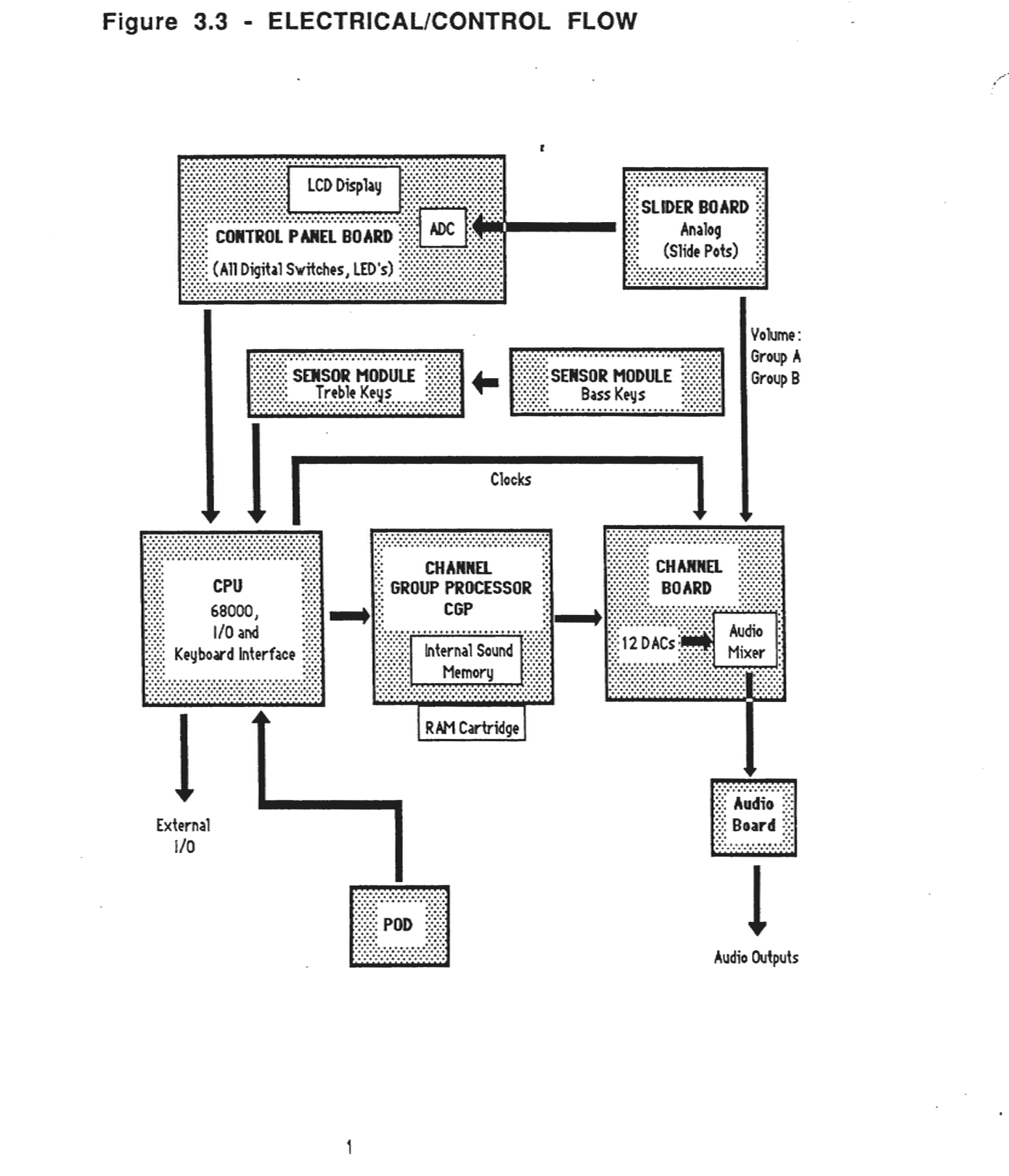
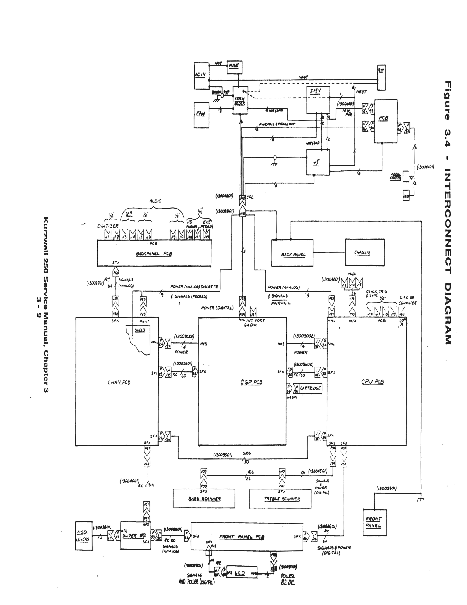
Figure 3-4 - INTERCONNECT DIAGRAM
3.4 - FUNCTIONAL DESCRIPTIONS
3.4.1 - CPU (Central Processing Unit)
The "Central Processing Unit" (CPU) board controls the operation of the entire system. It controls all I/O; reads data from the keyboard and the Front Panel, directs the dialogue on the LEDs and LCD display, controls the bi-directional personal computer port, and handles MIDI In, Out and Thru. The CPU board also tells the other two boards when to generate sounds, and it coordinates the signals on the various connectors on the back panel.
The CPU board contains the following hardware:
*68000 microprocessor
*PROM bank
*RAM bank
*PROM-or-RAM bank
*Interface to Front Panel
*Music Keyboard scanner with interface to keyboard
*Interface to Personal Computer
*MIDI interface
*24 16-bit programmable timers
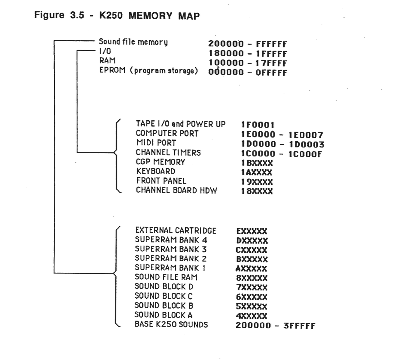
Of the 16 megabytes of memory addressable by the 68000, the first 2 Mbytes are reserved for system memory and I/O. The remaining 14 Mbytes are reserved for sound file memory located external to the CPU board, on the Channel Group Processor board (CGP).
The CPU board's internal bus is not accessible to the Channel Group Processor (CGP). Instead the CGP talks directly to sound file memory over its own bus. The CPU communicates with the CGP over a special interface bus. It has access to the sound file memory, but under control of the CGP.
The CPU board also contains the hardware for handling the 88-note keyboard, including switch debounce circuitry.
68000 and Memory
RAM - The K250 has 128 Kbytes of memory. The memory is allocated for the system's use and for sounds.
PROM - The software that controls the K250 is built into PROM. There are 8 system PROMs on the CPU board. Two of these are replaced when the Diagnostic PROMs are used. Each PROM is labeled with a sticker that indicates its location in the bank of PROM, and a checksum value. Every version of the software will have unique checksums associated with it.
Battery-Backed Memory - The CPU board contains a battery which provides power to retain memory after power down. This Battery-Backed memory saves keyboard setups and other user information.
I/O Ports
MIDI - The MIDI port is a 68A50 serial port.
MIDI IN - This is a 31.2K baud, 5 milliamp serial input.
MIDI THRU - This is a 31.2K baud, 5 milliamp serial output.
MIDI OUT - This is a 31.2K baud, 5 milliamp serial output, the same as MIDI In buffered, conforms to MIDI specifications.
Computer Port - This port is for attaching a personal computer to the K250. The K250 Personal Computer I/O Port currently uses the Apple Macintosh's serial signalling convention.
Trigger In - The Trigger In is a TTL-compatible input used for starting a sequence from an external device. The sequence triggers on the positive edge of the supplied pulse. Minimum pulse width is 1 microsecond. The input impedance is greater than 10k ohms. The trigger level is 2 volts. This I/O port takes a 1/4 inch phone jack.
Click Out - The Click Out is a TTL-level output pulse. When enabled from the Front Panel, a positive pulse appears at this output. Its repetition rate is the selected sequencer tempo. Driving source is a low power TTL gate through a 51 ohm resistor. This I/O port takes a 1/4 inch phone jack.
Sync In - The Sync In is a TTL-compatible input used to drive the K250 from another instrument. The other instrument is to provide a square wave at X12 to X96 the tempo. The input impedance is greater than 10k ohms. The trigger level is 2 volts and this I/O port takes a 1/4 inch phone jack.
Sync Out - The Sync Out is a TTL-level square wave output used to drive another instrument in synchrony with the K250. The repetition rate is normally X12 to X96 the tempo. The driving source is a low power TTL gate through a 51 ohm resistor. This I/O port takes a 1/4 in phone jack.
LO - These are 2.6, absolute maximum, VPP audio outputs, with a 600 ohm driving source impedance. Typical output levels are an order of magnitude lower than maximums. These require 1/4 inch phone jacks and are suitable for line level inputs.
HI - These are 26, absolute maximum, VPP audio outputs, with a 600 ohm driving source impedance. Typical output levels are an order of magnitude lower than maximums. These require 1/4 inch phone jacks and are suitable for directly driving power amplifiers and other high level inputs.
Balanced - These are 26, absolute maximum, VPP audio outputs. They have XLF connectors, floating outputs and a 600 ohm driving source impedance. Typical output levels are an order of magnitude lower than maximums.
External Pedals 1 and 2 - The 1/4 inch phone jacks accept external pedals.
MIC - This digitizer input is a 200 mVPP full scale input. It has a 47K ohm input impedance and accepts a 1/4 inch phone jack.
Line In - This digitizer input is a 1 VPP full scale input (300 mV rms). It has a 10K ohm input impedance and accepts a 1/4 inch phone jack.
Front Panel Control Interface
The Front Panel Control Interface circuitry is located on the CPU board. It consists of an 8 bit bi-directional data port, and eight control lines. The CPU communicates with the control panel through the data port. The Front Panel Control Interface consists of:
*LCD Interface
*Switch/LED Interface
*A/D Interface
Keyboard Interface
The Keyboard Interface is on the CPU board. It detects "events" happening at the keyboard, and reports information about them to the CPU. Since the CPU may not be able to respond to events immediately, data is saved until ready for use. An event may be either an "attack" (key depression) or a "release" (key released).
When the machine is first plugged in, the keyboard controller assumes that all the keys are "at rest". It then requests the keyboard sensor modules to examine each key 4000 times per second. As long as a key remains "at rest", the sensors activate the "Kr" signals when the key is examined. The key is said to be "at rest". When a key is pressed down, though, "Kr" is no longer activated. If it is pressed down for long enough, the "Kd" will be activated but this does not happen right away, so for a while neither the "Kr" nor "Kd" is active.
As long as neither "Kr" or "Kd" is active, following "rest" the key is said to be in the "falling" state.
When "Kd" finally becomes active, the key is said to have entered the "down state". At the same time, an "attack event" is reported to the CPU. This report includes a flag identifying it as an attack, the key number and its time of flight. Time of flight is used to determine how hard a key was pressed.
A counter exists for each key. Whenever a key is in the "rest state", its counter is reset to zero. While a key is in the "falling state", its counter is incremented every quarter-millisecond. As soon as the key enters the "down" state, the accumulated count is reported (in inverted form) as velocity. It shows how many quarter-milliseconds the key took to fly between "rest" and "down" state. A "release" is essentially a mirror image of an attack. When "Kd" ceases to be active, the key enters the "rising state" and its counter starts incrementing every quarter-millisecond. As soon as "Kr" becomes active again, the count is reported as time of flight, tagged as a "release event" and the key re-enters the rest state.
Figure 3.5 - K250 MEMORY MAP
3.4.2 - Channel Group Processor (CGP)
The Channel Group Processor (CGP) board acts an intermediary between the CPU and channels. It has, in a large memory, definition for all the sounds the instrument can produce. On command from the CPU, it will send any sound in the memory to designated channel (or multiple sounds to multiple channels).
The soundfile memory is a dual-ported, dual-mode array of memories which have a maximum of 14 Megabytes of total address range. The two ports are the CPU and the CGP. The two modes are sound and data.
The CGP performs four functions:
1. Fetching (DMA) sound samples from main memory
2. Buffering of up to 16 sound samples in (FIFO)
3. Servicing of requests for sound samples from up to 12 channels (one per sampling clock tick)
4. Interrupting the main process at the end of each waveform, under microprogram control
Each port has its own address strobe (CGAS/ for the CGP, SFAS/ for the CPU). This indicates to the memory controller PAL that a request is pending, and will initiate arbitration of the soundfile memory. In both devices, the request will remain stable until an acknowledge (SFACK/ is given to the appropriate device. If no request is active, the controller PAL will initiate a RAM refresh cycle.
The two address busses are tri-state multiplexed onto a common Soundfile Address bus (SFADDR). The buffer enables are tied to CPSFIP/ and CGSFIP/. When arbitration has occurred, these signals indicate access to soundfile memory, and 50 ns. is allowed for the signals to settle on the SFADDR bus. On the next cycle RAS/ will always go low, which signifies that the addresses are valid, and the access time of the memory begins (usually 250 to 350 ns.). During the RAS/ state, we require that the memory control signals such as read/write and SOUND, the mode control, become valid. This allows the data paths to be set up in the appropriate way, as well as the special circuitry required to generate the SOUND samples. Depending on the memory type (shown in figure 3.5) and the setting of the DTACK jumper, this may also generate DTACK/ to the requesting device. The next cycle, CAS/ is generated only if the RAM was accessed. There are actually 4 CAS/ signals, corresponding to UDS/, LDS/, SOUND*UDS/, and SOUND*LDS/ (CASH/, CASL/, SCASH/ and SCASL/).
The main soundfile data path (SFDATA), is used for both sound and data. The CPU selects the mode it wishes to access soundfile memory by writing to two locations in the CGP address while RDSOUND changes back into data mode. Both of these accesses have no wait stages. When the CPU accesses sound, each sample appears to occupy a single byte (this so that the soundfile can have uniform addressing, and word transfers can occur in one cycle). This means that the 68000 must pre-store the 2 LSBs of the sound in a special latch (called, not surprisingly, the Sound Latch) before doing a write to sound memory, and this is accomplished whenever WRSOUND occurs. The reading of soundfiles is done by writing WRSOUND, performing a soundfile access, and then extracting the 2 LSB's by reading RDSOUND.
The 12 channels operate independently in all of the above tasks, and are time-multiplexed using high-speed (10MHz.) dedicated logic. Before a channel may be enabled, the appropriate parameters must be loaded by the main CPU into the CGP Local Memory. In addition, the individual channel must be set up to generate the appropriate amplitude, Sampling clock and Anti-Alias clock rate.
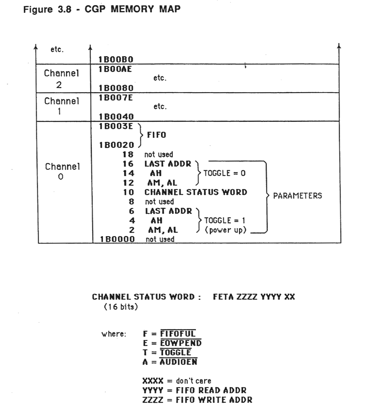
We begin our description with the programming sequence required to initiate a sound in the CGP. In the Kurzweil 250, only 12 channels of the possible 16 channels are provided. Each channel has an on/off hardware control located in the Channel Enable Word (CEW). This bit must be off (0) before channel initialization begins. Then, we write the CSW with all 0s which performs the following functions:
1. Initializes the FIFO write and read pointers to FIFO location 0. 2. Sets the "FIFOFULL" bit to 0, indicating that the FIFO is not full, and should be filled the first time the channel is polled. 3. Clears the "End-of-Waveform Pending" and "Audio Enable" bits (described later). 4. Sets the "Toggle" bit to point to the lower span.
Once the CSW is initialized, it should not be re-written until the channel has been de-allocated, because the parameters are modified as the sound progresses.
Next, two spans should be loaded into the appropriate locations of the CGP, the lower one being first, followed by the higher one. Note that the span has a maximum length of 64K samples, and may never cross a 64K boundary. When the appropriate sampling and alias clocks and amplitude DAC have been initialized, the channel can be enabled by writing to the CEW.
First, we will describe a typical life of a waveform. We begin with setting up all of parameters described above. When all is ready, the channel in question is enabled by writing to the appropriate bit in the Channel Enable Word. On the subsequent 16 polls of the enabled channel, the CGP will perform a DMA cycle to fetch a sound sample pointed to by the DMA HIGH and DMA LOW parameters in the CGP parameter memory. This DMA address is then incremented and written back into the CGP local memory, compared with the DMA LAST. The sound sample is also written into the CGP local memory in a special location dedicated to this channel's FIFO. The pointer address to the channel's CGP FIFO pointed to by a field in the CHANNEL STATUS WORD (CSW). This word is updated every time the FIFO is written to or read from. The CSW is written into only once, when the channel is being initialized.
Sixteen such DMA operations will occur in succession, until the FIFO is filled. At this point, the sampling clock will be enabled (free running mode). Nothing will happen until the first sampling clock tick occurs, which signifies that a sound sample is requested at the Signal Channel Data in the channel. The CGP simply pops the first FIFO'd sample onto the DAC BUS, updates the CSW (now indicating that the FIFO is not full), and proceeds to the next channel. On the next poll, the CGP will perform another DMA operation to keep the FIFO full.
Another function concerns when the DMA address matches the micro-programmed DMA LAST ADDRESS. This will generate a vectored interrupt of the main CPU, and invert the TOGGLE BIT, which points to one of 2 sets of parameters which the CGP processes. In this way, the DMA operation is not stopped at the end of each waveform, the main CPU has one full waveform to update the other parameter set in the CGP local memory.
If an interrupt has been generated by one channel, and another channel also reaches the End-of-Waveform before the first interrupt has been serviced; a bit is set in the CSW and the interrupt is issued on the next DMA cycle in which an interrupt is not pending.
Finally, when the amplitude of the signal has been ramped down to inaudible, the channel may be de-allocated by writing a zero to a bit in the Channel Enable Word.
Now, we can look at the CGP State Diagram (figure 3.7) to trace the cycle by cycle operation of the CGP. On RESET/, the CGP is initialized to state 0, then it unconditionally jumps into state F, which increments the Channel Count (CHCNT), which will be stable before the end of state F. In addition, the CPU may want to access the Group Processor, so that if CPGPRO/ is active, State F is when the CPU-Group Processor communication occurs (CPGPIP). When the access is complete, or if no access occurs, the CGP reads the CSW in State D. The status should be latched and stable by the end of this clock cycle. The appropriate bit of the CEW which determines the Channel Enable (CHEN) should also be present at the PAL input, and determines whether the CSW should be ignored (State F) or looked at (State 3).
In the Decision state, we discover (via the CSW) whether the FIFO is full (FIFOFUL), whether the channel (via the Channel board) is requesting a sample (CHRDRQ), and whether the 68000 is currently accessing soundfile ROM. Anytime the FIFO is not full, the CCP performs a DMA from soundfile memory to the FIFO, however it may have to wait for the CPU-soundfile transfer (CPSFIP) to complete. If the channel is requesting a sample, it can service this request during a DMA cycle, or to State 5 if the FIFO is already full.
Figure 3.6 - CGP BLOCK DIAGRAM
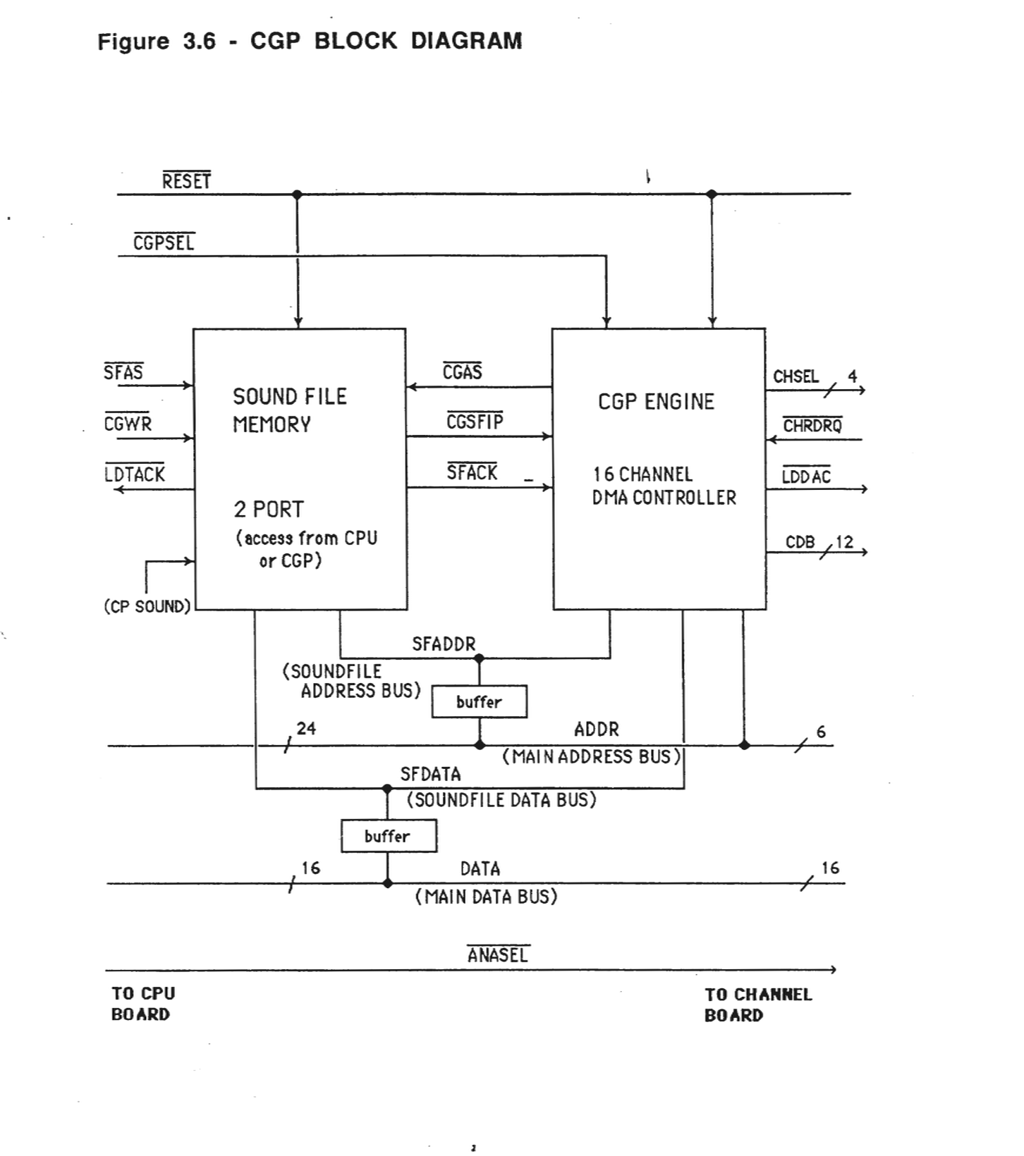
Figure 3.7 - CGP STATE DIAGRAM
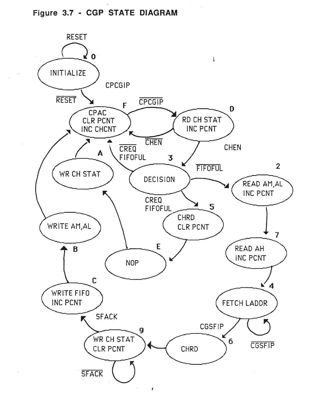
Figure 3.8 - CGP MEMORY MAP
In State 5, the CGP memory is addressed by appending the channel number (CHCNT), and the FIFO read pointer to fetch the appropriate sound sample, and latch it into a buffer for transfer to the Channel board. Next, we increment the FIFO read pointer, and compare it to the FIFO write pointer. If they are equal then the new FIFO full is asserted, and the new CSW is written over the old one.
If a DMA cycle is required, the sequence is as follows:
1. Read and latch the low 16 bits of the DMA address.
2. Read and latch the high 8 bits of the DMA address. Also assert CGP address strobe (CGAS).
3. Perform a Channel Read, if required (identical to State 5).
4. Read, latch and compare the programmed last address (LADDR) with the current DMA address
5. Rewrite the CSW, incrementing the FIFO write pointer, the FIFO read pointer (if necessary), and updating FIFOFUL.
6. Write the new sound sample into the CGP at the address pointed to by the FIFO write pointer.
7. Write the new DMA address for the channel (old one +1) over the old one.
In this way, the CGP attempts to keep all of the active FIFO's full, while guaranteeing one-poll service of channel requests.
The other interface requirement is that of the Last Access (LAST), which performs the following functions;
1. Inverts the Toggle bit of the CSW, which points to the current active span parameters. 2. If there is no interrupt pending, the current channel number (CHCNT) and a single bit (UPDATE) are latched into a buffer for examination by a CPU. The format of the Vector byte is:
VECTOR: | 0 0 | D C B A | U | 0 | CHCNT UPDA
The CPU is then interrupted (level 6) and must read the contents of the vector to determine which channel and which span to update. This also clears the interrupt. During the time between the interrupt and the reading of the vector, End-of-Waveform in Progress (EOWIP) is set.
If there is an interrupt pending, the current CSW is modified to have its End-of-Waveform Pending (EOWPEND) bit set. This is examined every time the CSW is read, and if active, the EOWIP signal is sampled to determine whether the current EOWPEND can be made active ("peeled") or remain pending. The vector and EOWPEND bit are adjusted accordingly.
How to operate a channel
1. Set up sampling and alias clock rates
write to 8254 control location
write 2 bytes to each clock location
2. Set up parameter block in CGP local memory
write channel status word 0 x FFFF
write DMA starting location (AM, AL)
write DMA high order address, interrupt vector
write DMA last address
3. Write to appropriate amplitude DAC
4. Enable channel via channel control location
To disable a Channel
1. Make sure AMP DAC is at minimum amplitude
2. Disable channel via channel control location
3.4.3 - Channel Board
The actual generation of sound is performed by the Channel board. Each of the 12 channels on it can create different arbitrary sounds, all of which get mixed together into two audio outputs. These outputs are sent to an external amplifier and speakers via the Audio board.
As shown in the drawing, K250 Channel board (figure 3.9), the Channel board has several subsections of circuitry. The block on the right hand side of the board is labeled CGP/Channel interface. The section of the circuitry controls the flow of sound samples in an orderly manner from the CGP to each of the 12 channels on the Channel board. Each channel must receive its sound samples in exact synchronizim with the channel timers located on the CPU board. Since the K250 is a variable sampling rate instrument, each channel may be playing out a sound at a different sample rate. There are two sets of signals which go from the CPU to the Channel board one labeled FSAMP and the other labeled FALIAS. There are 12 FSAMP signals, one for each channel and 12 FALIAS signals, one for each channel. These 24 signals come over the long flat ribbon cable from the CPU board to the Channel board directly.
These two sets of signals are generated by the 24 programmable timers located on the CPU board. The clock rate for each FSAMP signal is precisely the sampling rate of that particular channel. The CGP is designed to deliver samples just as fast as the Channel board can call for them for each of its channels. Therefore, this section of circuitry could be thought of as a section which trottles the flow of samples to each channel. The middle section of the board is actually where the 12 identical channels reside. All channels are identical except channel 12. Channel 12 varies slightly from the other 11 in one respect. Some of Channel 12's circuitry is used for the sampling function.
The output of each of the 12 channels is then fed into a stereo mixer section on the left hand side of the Channel board where the 12 channels are mixed into 2 channels. Driver amplifiers in this section of circuitry amplify the left and right signals and feed them to the output connector which goes to the Audio board.
This section circuitry also controls the 12 groups select switches for switching each channel's sound onto either an A BUS or B BUS. The audio board which attaches to this connector holds primarily the audio outputs jacks. On the Audio board is also a preamplifier circuit used the Channel board. The external pedal inputs come in over this connector and are routed through the Channel board to the connector at the bottom of the Channel board which goes to the Slider board. Coming from the Slider board to the Channel board are the signals which control the left/right balance, the audio outputs.
A typical channel is diagrammed in the drawing, Analog/Channels Block Diagram (figure 3.10). On the left-hand side of the diagram is a BUS called DATA, this is a set of 16 data lines which come directly from the CPU board.
The three sets of signals labeled DATA, FALAIS and FSAMP come directly from the CPU board, whereas a set of signals labeled CDB BLU come directly from the CGP board. These 12 lines labeled CDB carry the actual sample data from the CGP to the Channel board. Samples are stored in 10-bit format so the bottom 2 bits of this 12-bit bus always contain zeros. The design of the K250 attempts to maximize the signal to noise ratio by keeping the actual sample data as close to full scale as possible at all times, and having the decay information in the sound contained in an envelope control section. By way of example, consider the Kurzweil Grand Piano sound. When a note is struck, as the sound dies away, the sound samples themselves are kept as close to full scale as possible and the ramp down of the sound is caused by the envelope ramping down. Each channel has a 8-bit DAC which serves as the envelope control.
As sample data is being fed from the CGP, amplitude envelope information is being fed simultaneously from the CPU. The update rate of the amplitude envelope control information is much slower than the actual delivery of the samples from the CGP. Therefore, the CPU is fast enough to deliver this information in a timely manner. The amplitude envelope information for each channel comes in over the 16 data lines from the CPU. Actually, only 8 of these are used since the amplitude envelope control DAC is an 8-bit DAC. The output of this DAC, as seen on the block diagram, goes to the control input of the final VCA on each channel where the actual ramp down of the sound occurs on those sounds which decay.
The CDB BUS from the group processor feeds the sample information into each channel's 12-bit DAC. The output of the DAC goes into a sample and hold whose timing is controlled by the FSAMP signal which comes from the CPU board. The output of each sample and hold is fed into a very sharp cutoff low-pass filter called an alias filter. The function of the alias filter is to remove those components of the spectrum which are generated by the sampling process. As a channel finishes playing a note or sound a one sampling frequency, the next note that it receives may be at a different sampling frequency.
The frequency FSAMP changes to reflect the different sampling rates. Also the corner frequency of the alias filter changes to accommodate the new sampling rate. The output of the alias filter is fed to the output channel VCA, mentioned earlier, whose control input is driven from the 8-bit envelope control DAC. The output of this VCA goes to a solid state, SPDT switch. This switch switches the output of the channel onto either an A BUS or B BUS. The A output of each of the channels are all ganged into 4 additional VCAs. These VCAs control the relative balance of the A and B signals onto the left and right output busses. The control inputs to these 4 VCAs come from the Slider board on the front panel. At the top of the drawing labeled, Analog/Channels Block Diagram (figure 3.10), is a block called buffer. There are 12 outputs from this device; 1 for each channel. When a note is struck on the keyboard, the CPU after determining which note it is and various other parameters; determines whether the sound should be switched onto the A BUS or the B BUS. It does this switching before the sound actually starts.
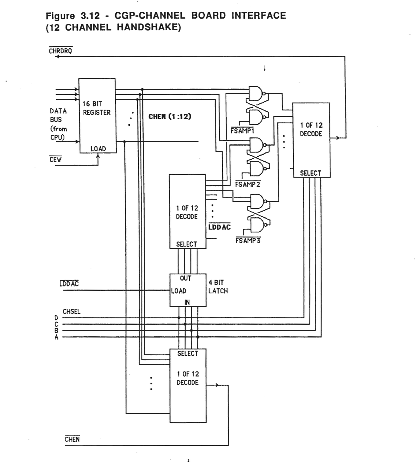
Refer now to the diagram labeled Handshake Diagram for a Single Channel (figure 3.11). As we mentioned earlier, the CGP can deliver samples generally much more quickly than the Channel board can take them. So the function of the interface circuitry on the Channel board is to throttle the delivery of the samples to each of the channels. It effectively does this throttling through the 12 signals labeled FSAMP. Imagine for a moment that the K250 is a 1 channel instrument while looking at this diagram. The signal labeled LDDAC stands for Load DAC Not and is the signal which eventually causes the signal DAC for this channel on the Channel board to be loaded with a sound sample. Once the CGP has been told by the CPU to start playing out a particular sound were it not for the throttling effect from the Channel board, the CGP would just spit out samples in rapid fire succession to the Channel so the LDDAC signals would be happening in rapid succession.
Imagine for a moment that the output of the box called 1-bit register is always high. So that the cross coupled gate flip-flop simply flips back and forth in response to the LDDAC and the FSAMP signal. The output of this cross coupled gate flip-flop is called CHRDRQ which stands for channel read request. It is this signal CHRDRQ which signals the CGP that the channel is ready for a new sample. Whenever this line goes low the CGP will then begin the process of loading a new sample into the channel.
But this signal CHRDRQ will only go low in response to the FSAMP input going low, but this is precisely the time when you want the sample to be delivered. That is, in synchronization with the FSAMP signal. Once that sample has been loaded into the DAC by the LDDAC pulse, then this same signal LDDAC sets the cross coupled gate flip-flop to the other state and causes CHRDRQ to go high. When the CGP sees the signal CHRDRQ go high, it will deliver no further samples until CHRDRQ goes low again, which will happen only when the next FSAMP pulse goes low. It is in this way that the sampling clock or FSAMP throttles the loading of the sampling information into channel. This all assumes that the output of the 1-bit register is always high. This would be the case if the channel is turned on. If that channel is not turned on, that is, not intended to play any sound, then the output of this register will be low by forcing the signal CHRDRQ to always reside high, which then causes the CGP to not load samples into that channel.
The channel is turned on or off by the loading of a 1 or 0 into this 1-bit register. If a 1 is loaded the channel will be turned on, if a 0 is loaded the channel will be turned off. This register is loaded at the beginning of the sound, right after the note is struck at the performance keyboard. When the note has finished playing out, then this register will be written from the CPU with a zero, which then turns off that channel. The 1-bit register for each channel goes to one line of the set of signals called DATA which come directly from the CPU board. DATA line 0 controls the turning on and off of channel 1, the 1 controls channel 2, 2 controls 3, etc.
The diagram labeled, CGP-Channel Interface (figure 3.12), shows how this simple single channel interface is used to service all 12 channels. The CGP only gives the illusion that all 12 channels are being loaded simultaneously. Each channel is actually being loaded one after the other in a round robin fashion. This sequential loading happens at a rate high enough to be indistinguishable from simultaneous loading of the channels. The set of four signals called CHSEL A, B, C and D determines which channel is to be loaded with a sample of information at any point in the cycling of the channels. The signal labeled CEW controls the turning on or turning off of each channel at the appropriate time. Through loading each channel with a either a 1 or 0 from the respective line from the DATA BUS. CHEN is a signal which is fed back to the group processor for its own use in determining whether a particular channel is on or off, as that channel reaches its turn in the continual cycling of the 12 channels.
Figure 3.9 - K250 CHANNEL BOARD
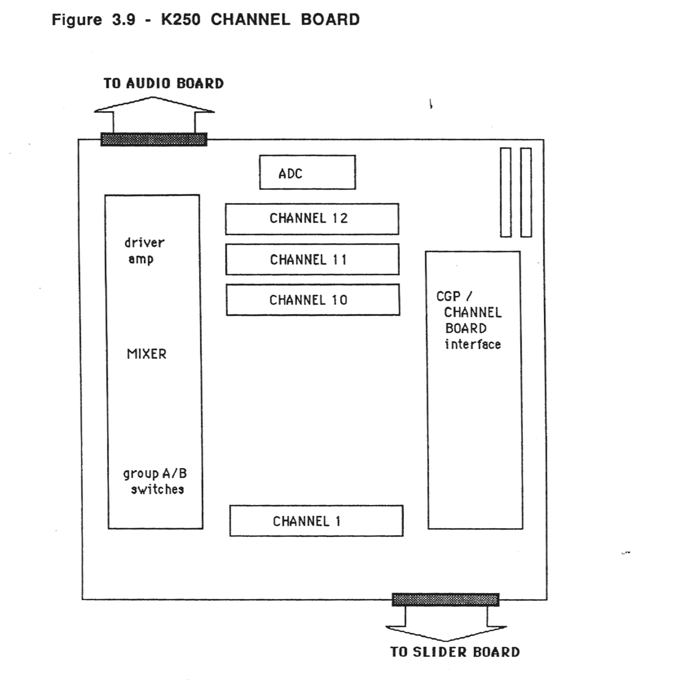
Figure 3.12 - CGP-CHANNEL BOARD INTERFACE (12 CHANNEL HANDSHAKE)
3.4.4 - Front Panel Assembly
The Front Panel assembly is hinged to open upwards for servicing. The faceplate silk-screening identifies each control. The three circuit boards, Control Panel, Display and Slider boards are attached underneath. The Control Panel board contains mostly digital circuitry and the Slider board contains mostly analog circuitry.
The Display board consists of the liquid crystal display unit (LCD) and its circuitry. The display shows numbers and text, letting the user carry on a "dialogue" with the instrument. The LCD shows two lines of 24 characters each. Any letter, number or punctuation can be shown. The display is used when a more elaborate message is needed than a flashing lamp can convey.
Control Panel Board
The Control Panel board is controlled and monitored by the CPU board. The signals from the CPU are decoded to see which sub-system (switches, lamps, LCD, etc.) is to be activated.
The Control Panel board also contains an "analog-to-digital converter" (ADC). This translates analog voltage levels into 8-bit binary digital values.
The main functions of the Control Panel are:
1. Control the LCD display
2. Control the LED's
3. Control the switches
4. Convert A/D
The "switch matrix" contains 55 pushbutton switches, used to enter numbers and predefined commands into the machine. Of these switches, 38 contain "light emitting diodes" (LED's) which form the "lamp array". These lamps are lit for various purposes such as a confirmation of actions or an indication of next possible actions.
The Control Panel board receives power and signals from the CPU through its connector. Power comes in on multiple wires to allow more current to flow. This also provides redundant contacts, increasing reliability. Most signals have either power or ground lines between them to reduce crosstalk.
Slider Board
The Slider board contains seven slide potentiometers which affect the instrument's tuning and other characteristics. It conditions and passes on signals from two "special-effects" levers, the two piano-type foot pedals in the POD, and two (optional) special effects pedals that plug into the back panel.
The Slider board provides analog signals:
1. to the Control Panel board for control of playing parameters (pitch, vibrato, etc.) 2. for the audio mixer on the Channel board, for controlling the audio output (loudness and balance) 3. for the two pots used to trim the Mod Lever
The Slider board is mounted on the left (bass) side of the front panel. It connects to three places:
1. through P51, carrying power from the signals to the Channel board 2. through P50 delivering power and signals to the Front Panel 3. through P41 from the Mod Levers
Display Board
The LCD display receives signals and power through connector P43. A bias voltage is applied to set the display's contrast and viewing angle. This voltage is adjustable with a pot which is accessible through a small hole (remove hole plug) in the Front Panel to the left of the keypad.
3.4.5 - Keyboard Sub-Assembly
The keyboard sub-assembly consists of the mechanical key actions (with wooden piano keys) and the two Scanner boards. The keyboard interface circuitry is on the CPU board and is described under that section.
Each of the 88 keys pivot on a rail running across the center of the keybed. When the "head" of the key (the black or white part) is pressed down, the "tail" (opposite end) rises. All the keys are weighted so that they normally rest with the tail end down.
When the tail rises, the action pivots upwards. A pin on the action activates a sensor. Each key has a corresponding sensor which is stationary with respect to the keybed.
Figure 3.13
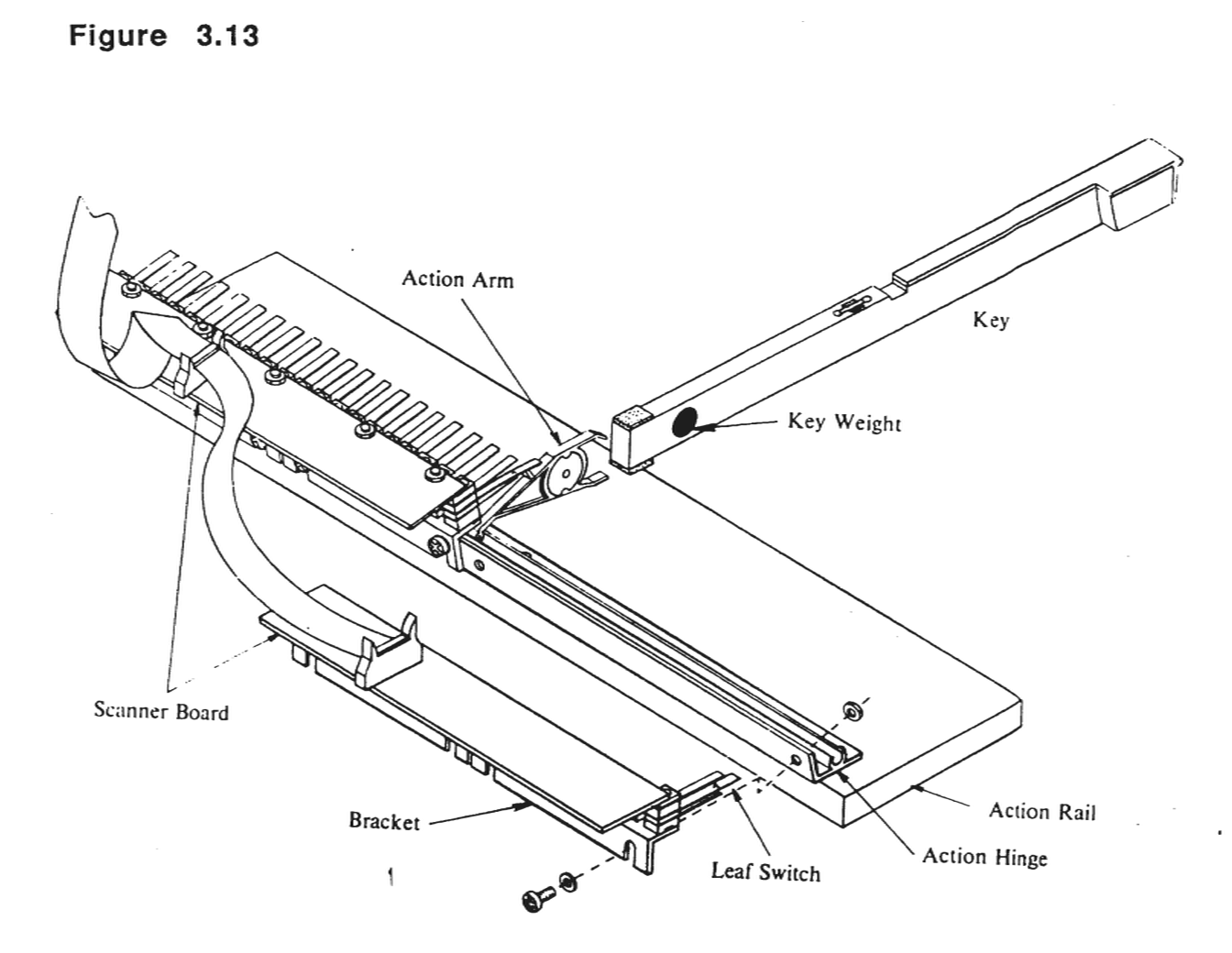
These sensors are leaf switches. They have a flexible inner "leaf", separated by spacers between two rigid outer leaves. The leaves are conductive. Normally, the center leaf touches one of the outer leaves making electrical contact. The action pin pressing against the center leaf moves it to the other contact. This changing electrical contact is used to determine when a key has been pressed.
Since the outer leaves are separated by some distance, it takes the center leaf a while to move from one contact to the other. This "time of flight" may be measured to see how hard the key was pressed. A key pressed softly takes a relatively long time to move the center leaf and make contact with the upper leaf, and conversely, a key pressed hard takes a short amount of time. This is called "velocity sensing". The K250 uses velocity sensing to express loudness, timbre and other aspects of the sound.
The standard spacing of the sensors is determined by piano-making convention. The standard "octave span" (width of 12 keys) on a piano keyboard is 6.5 inches. This is about 0.54 inches per keys. All 88 keys together span 47.5 inches. Since this is too large to economically put on one circuit board, the sensors are put on two modules each 24 inches long. One handles the bass keys (left half of the keyboard) and the other monitors the treble (right half).
3.4.6 - Keyswitch Boards
The CPU sends out a binary number pointing to the key to be examined. The sensor modules decode this and return a code representing the position of that key (up, down or in transit).
The 88 keys on the keyboard are normally stamped with a number on the top of the wooden lever. These numbers range from 1 (at the extreme left, or bass end) to 88 (at the right or treble end). They ascend in sequence from left to right.
3.4.7 - Audio Board
The Audio board functions simply as a distribution panel. The Audio board takes the two outputs from the Channel board's mixer and sends them to external audio connectors.
3.4.8 - POD Assembly
The POD assembly has been changed since the Kurzweil 250 was originally introduced. The original POD did not have a power supply that was switchable for different voltages. Therefore, the internal design for the PODs is quite different. The only design difference between the Kurzweil 250 and the Kurzweil 250X POD is that the Kurzweil 250X POD does not have pedals. The power supply board for the Kurzweil RMX is internal to the unit.
The following is a list of the part numbers for the different Kurzweil 250 and Kurzweil 250X PODs:
10000301    110V/120V, Kurzweil 250 POD

10000302    220V/240V, Kurzweil 250 POD

10002201    110V/120V, Kurzweil 250X POD

10002202    220V/240V, Kurzweil 250X POD

10002501    Switchable Kurzweil 250 POD

10003001    Switchable Kurzweil 250X POD
The bulk of the POD is the power supply. It contains a 5 volt supply for the system's logic circuitry, and a ± 15 volt supply for the audio circuitry. The newer, switchable POD contains only one board.
Another sub-system in the POD is a pair of piano-style pedals for controlling characteristics of the sound (such as whether notes are sustained after key release). The pedals are monitored by a circuit on the "POD board" which sends signals up through a cable to the main enclosure. These signals denote whether a pedal is up, down or in transit.
The POD assembly also contains circuitry which monitors the AC power line and produces an "advance warning" of imminent power failure. This circuitry is contained on the POD board in the older, non-switchable POD assembly. When this pulse is detected, the instrument saves information about its current state so that it can resume after power interruption.